In this lab, you will design more elaborate data paths and the handshaking to control them. You will use a VHDL test bench to test the design in simulation.
You may work on this lab alone or in groups of two.
Make copies of these files in your ece511/lab4 directory:
adder.vhd
adder_pkg.vhd
adder_test.vhd
lfsr_generic.vhd
Start a new project and add adder.vhd, adder_pkg.vhd and adder_test.vhd.
Pre-compile lfst_generic.vhd and adder_pkg.vhd in your Xilinx project directory (work area)
% cd to_your_xilinx_project_directory
% vlib work
% vcom -93 -explicit ece511/lab4/adder_pkg.vhd
% vcom -93 -explicit ece511/lab4/lfsr_generic.vhd
A testbench (adder_test.vhd) that generates the test vectors and analyzes the results has been provided for your use. You will instantiate your adder as a component in this testbench to test your adder later in the lab.
Note, adder.vhd as provided, actually contains a pipelined XOR with insufficient handshaking.
Please note the following points about this design:
Back in Xilinx modify the properties of the post place & route simulation for adder_test.vhd. Set the UUT Device Instance to adder_part and the simulation time to 8000 ns. Run the post place & route simulation. Set the waveform output to hexadecimal.
www.opencores.org/projects/rs232_syscon/
www.opencores.org
| Hardware | WebDocs and Manuals | FPGA |
| Digilab 2 and D2IO board www.digilentinc.com
(also used in EE480) |
D2 Reference Manual (pdf) ,
D2 Schematic (pdf) , D2 IO Reference Manual (pdf) , D2 IO Schematic (pdf) , D2D2IO Pin Connections (pdf) , LCD KS0066U Controller (pdf) , |
Xilinx Spartan2 XC2S200 (Package: PQ208) |
In this exercise you will establish a serial connection between the PC, D2 board and the D2IO board. We will be using a VHDL conversion of OpenCores' RS232 System Controller (see the Module Contribution page).
Using the hyper-terminal program you will be able to read/write the push
buttons, switches, LEDs and seven segment display.
Download the design files - rs232D2IOwb.zip
Contains:
toplevel.vhd
- Instantiates rs232_syscon, a dual port memory and the wishbone interface
to the D2IO board
toplevel.ucf
- Connects top level signals to the right pins on the D2 board and D2IO
board (See the D2 Reference Manual
, D2IO Reference Manual for a list
of the pins)
rs232_syscon.vhd
-
The rs232 controller and Wishbone master
serial.vhd
- rs232 receiver and transmitter
D2IO_driver.vhd
- Access the hardware resources on the D2IO board
wbd2io.vhd
- a Wishbone interface for the D2IO board
dualportram.vhd - a 32 x 16-bit dual port memory
Create an new project and add the design files, including the toplevel.ucf pin map file, to your project. When Xilinx asks, associate the .ucf file with the toplevel design module.
In the Processes for Current Source window right click Generate Programming File and select properties. Goto Startup-Options and change the FPGA Start-Up Clock from CCLK to JTAG Clock.
In the Processes for Current Source window under Generate Programming File double click Configure Device (iMPACT).
Impact will bring up a pop-up window asking how you want to configure your device; choose boundary-scan. You can try to auto-detect the device. If the device it finds is not xcs2s200 you will need to repeat these step and specify a the boundary-Scan Chain (after selecting the boundary-scan to configure the device) as C:\Xilinx\Spartan2\data\xc2s200.bsd
Right click the Xilinx Chip and assign a new configuration file. Select toplevel.bit in your xilinx work area. Right click the chip again and select program.
The D2 board should now be programmed.
Connect a serial port cable between the host and the D2 board.
Click Start->Programs->Accessories->Communication->HyperTerminal. Ignore the error messages that pop up.
To configure the port settings make sure you are disconnected, then click File->properties. Click configure in the window that pops up. Change the settings (we used 9600, with no flow control, Data type of ANSI). click Ok.
Click the connect button.
Press return. 'Return' is the sequence of ones and zeros that the rsr232 system controller used uses to synchronize itself with the serial port baud rate.
If you see any recognizable characters in the HyperTerminal then it
is working. Look in the code comments to see how it works.
> w 0000 1234 -- writes 1234 at address 0000
> r 0000 -- read from address 0000
Address Map:
Address 0000 to 000F is internal RAM (read-write)
Address 0010 is the push buttons (read-only)
Address 0011 is the switches (read-only)
Address 0012 is the LEDs (read-write)
Address 0013 is the seven segment display (read-write)
Add a latch to the Wishbone rs232 D2IO controller that controls the state of LED1 on the D2 board. The LED should turn on when a '1' is written to address 0020 and turned off when a '0' is written.
The LED controlled by pin 71.
Demonstrate a latched controlled LED to the TA.
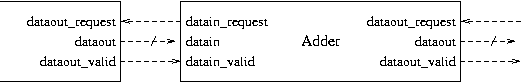
The pipeline must stall when dataout_request goes low. However, any stages containing invalid data as determined from datain_valid must not stall. The result will be that valid data already in the pipeline must not be lost. Invalid data in the pipeline however, should be flushed.
Use the following handshaking signals shown in the diagram below.
Your entity should be compatible with the component definition in adder_pkg.vhd.
Measure the total number of logic cells in the design, the throughput and the latency. Throughput is the maximum clock frequency (MHz) multiplied by the number of output bits. We will define latency as the number of pipeline register stages, not counting the first one, times the minimum clock period.
Supply the following:
You do not have to write a testbench as long as your adder.vhd is compatible with adder_pkg.vhd. Simply compile and simulate as in Exercise, Part B.
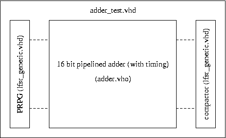
Synthesize your adder and generate timing-annotated VHDL output (see exercise and instructions above). For your simulations, use the provided stimulus signals in adder_test.vhd. This uses initial seed values for the pseudo-random generators. Run your simulations for at least 8000 ns. Use a simulation resolution of 'ns'. Display only selected signals or else you will display thousands of signal traces internal to the design.
Here is what the testbench stimulus signals test:
a_internal
b_internal
seed_a
seed_b
sum_internal_x
signature_x
clock
reset
load_prpg
load_compact
serial_prpg_a
serial_prpg_b
serial_compact_x
datain_request_internal
dataout_valid_internal
dataout_request_internal
datain_valid_internal