The insulated-gate FET, also known as a metal oxide semiconductor field effect transistor (MOSFET), is similar to the JFET but exhibits an even larger resistive input impedance due to the thin layer of silicon dioxide that is used to insulate the gate from the semiconductor channel. This insulating layer forms a capacitive coupling between the gate and the body of the transistor. The consequent lack of an internal DC connection to the gate makes the device more versatile than the JFET, but it also means that the insulating material of the capacitor can be easily damaged by the internal discharge of static charge developed during normal handling.
The MOSFET is widely used in large-scale digital integrated circuits where its high input impedance can result in very low power consumption per component. Many of these circuits feature bipolar transistor connections to the external terminals, thereby making the devices less susceptible to damage.
The MOSFET comes in four basic types, N-channel, P-channel, depletion
and enhancement.
The configuration of an N-channel, depletion MOSFET is shown in
figure 5.19a.
Its operation is similar to the N-channel JFET discussed previously: a
negative voltage placed on the gate generates a charge depleted region
in the N-type material next to the gate, thereby reducing the area of
the conduction channel between the drain and source.
However, the mechanism by which the depletion region is formed is
different from the JFET.
As the gate is made negative with respect to the source, more positive
carriers from the P-type material are drawn into the N-channel, where
they combine with and eliminate the free negative charges.
This action enlarges the depletion region towards the gate, reducing
the area of the N-channel and thereby lowering the conductivity
between the drain and source.
For negative applied gate-source voltages the observed effect is
much like a JFET, and ![]() is also about the same size.
is also about the same size.
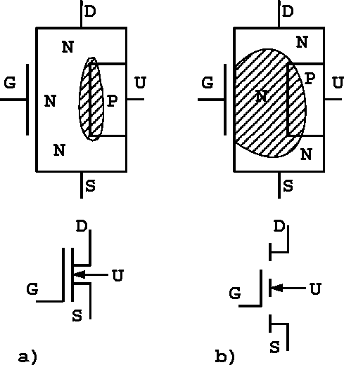
Figure 5.19: a) Depletion or depletion-enhancement type
MOSFET and b) enhancement type MOSFET.
However, since the MOSFET gate is insulated from the channel, positive gate-source voltages may also be applied without losing the FET effect. Depending on the construction details, the application of a positive gate-source voltage to a depletion-type MOSFET can repel the minority positive carriers in the depleted portion of the N-channel back into the P-type material as discussed below, thereby enlarging the channel and reducing the resistance. If the device exhibits this behaviour, it is known as an enhancement-depletion MOSFET.
A strictly enhancement MOSFET results from the configuration shown in figure 5.19b. Below some threshold of positive gate-source voltage, the connecting channel of N-type material between the drain and source is completely blocked by the depletion region generated by the PN junction. As the gate-source voltage is made more positive, the minority positive carriers are repelled back into the P-type material, leaving free negative charges behind. The effect is to shrink the depletion region and increase the conductivity between the drain and source.