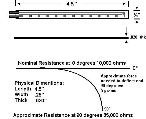
The Flex Sensor is a unique component that changes resistance when
bent. An unflexed sensor has a nominal resistance of 10,000 ohms (10 K).
As the flex sensor is bent the resistance gradually increases. When the
sensor is bent at 90 degress its resistance will range between 30-40 K
ohms.
![]()
The sensor measures 1/4 inch wide, 4 1/2 inches long and is only .019
inches thick.
The flex sensor perceives changes in bend angle as a linear proportional
change in current or voltage. Different flex angles cause the area of the
resistor to differ from its un-flexed 10K value ,resulting in this characteristic.
The bending of the sensor is registered as a change in resistance only
when the sensor is flexed in one direction (out of the screen in relation
to the picture at the top of screen). There are two simple configurations
of the flex sensor circuit:
1. Voltage divider: allows you to measure a changing voltage due to a change in the bend angle (the one used in the demo circuit)
2. Voltage divider, followed by a voltage to current converter (op-amp),
so that the flex can be measured in terms of current.
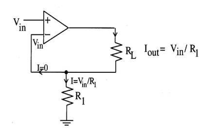
Voltage to Current Converter circuit.
Some appications for the Flex Sensor are:
Sign Language Translation Glove
Collision detection on mobile robots
VR Gloves and VR suits
Physics applications and experiments
Medical Devices for measuring heart beat etc.
Flex Sensors cost approximately $10 each plus shipping and handling
(only available from the US- JameCo
)
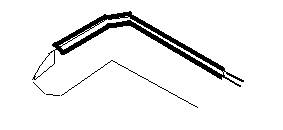
The flex sensor is ideal for any project where precise measurement of the motion of a particular component is required. It should be placed across the area on which flex is to be measured (preferably across the area of maximum bend).
Flex Sensor placed on finger to measure the level of flex on the finger
(Utilized in glove to translate Sign language):
The reason that analog to digital conversion is required is so that the
changing voltage values due to bend, will be in a format (digital) which
the FPGA can utilize. Levels of motion can be mapped to these particular
voltages by characterizing the particular types/levels of motion with the
flex sensors in place and tabulating these voltages. If these tabulated
voltages are placed in RAM or FLASH memory they can be compared to values
measured continuously by the FPGA and therefore the level of motion will
be known. In our case we found it simplest to put the default sensor comparison
values in the on chip lpmRAM. Either a voltage sensitive or current sensitive
ADC can be utilized in design with flex sensors. Current sensitive ADC
can be more accurate, because it will allow more levels of flex to be measured
(A higher voltage can be tolerated in this circuit, because this voltage
will not be an input to the FPGA’s 5V maximum pins. However,
due to availability and necessity it may be easier to get a voltage sensitive
ADC. In the case of the sign language glove the number of levels
of flex using a voltage divider circuit was more than enough to differentiate
between each letter in the American Sign Language Alphabet.
In our case, Six flex sensors were integrated into a glove and connected
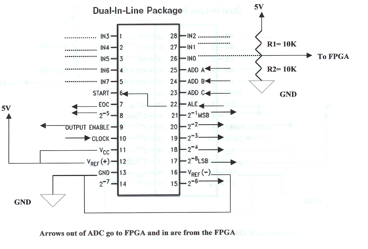
to the FPGA via the ADC
0809 (manufactured by National Semiconductor). The flex sensors were
connected to inputs IN0 ... IN5 with the voltage divider shown. The resistor
R1 is the flex sensor which starts at minimum bend with a resistance of
10 K.
The code included should be compiled in the order ADC_pkg.vhd, SLG_pkg.vhd, multiplex.vhd, nregister.vhd, enregister.vhd, debouncer.vhd, clk_divider.vhd, adconverter.vhd, ADController.vhd. The pinouts, which will be relevant for the Altera Exalibur board only are contained in ADController.csf. The above code will allow you to view the digitized flex sensor voltage of the sensor connected to IN0, but can easily be modified to rotate through up to eight flex sensors. The readings are displayed on the 7 segment LED, each segment representing a bit of the 8 bit output of the ADC. The enable/acquire button is used to start a conversion cycle and converts flex sensor voltages 0 through 5.
The clk_divider creates a 500kHz clock for the ADC and the debouncer
is used to avoid multiple ADC conversions per button push. Multiplexer
provides an enable for the n bit register which is put together in enregister.
These registers store the digitized voltage values, and a data_valid flag
is set once all six flex sensor voltages have been converted and registered.
Adconverter.vhd is controlled by the top level file ADController.vhd