The purpose of this lab is to introduce you to the Verilog HDL.
All synthesis and simulation will be done using Altera's MAX+PLUS II software,
using an EPF10K20RC240-4 device.
This lab has two parts: an exercise that is not handed in, in which you will become familiar with the tools, and a lab that will be submitted for marking, in which you will create your own design.
The MAX+PLUS II Verilog help is located under "Help" -> "Verilog HDL". This help is quite useful for beginners and it is recommended that you refer to it as you learn. Also, a number of useful templates can be accessed from the "Templates" -> "Verilog Template..." menu option. Between the online help and the examples provided, you will have enough Verilog knowledge to complete all parts of this lab. However, there are a number of good Verilog texts published if you want to learn more.
Although the coding standard provided to you in class is specific to
VHDL, it is expected that you follow a coding style as similar as possible
to the one provided, and that all code is understandable and adequately
commented (Verilog uses "C" style comments).
Verilog has many similarities to VHDL. In fact, most constructs are identical, only they have different syntax. However, there are still a number of differences. The biggest difference comes from the fact that VHDL is much more strongly typed than Verilog. Read through the following examples to get a feeling for the similarities and differences between Verilog and VHDL.
Entity/Module Declaration
| VHDL:
entity count is generic (counterwidth : positive := 32); port(enable, aclr, clock : in std_logic; q : buffer std_logic_vector(counterwidth-1 downto 0) ); end count; |
Verilog:
module count(enable, aclr, clock, q); parameter counterwidth = 32; input enable, aclr, clock; output [counterwidth-1:0] q; reg [counterwidth-1:0] q; |
Process Definition
| VHDL:
counter : process(clock) is begin if rising_edge(clock) then q <= q + 1; endif; end process counter; |
Verilog:
always @(posedge clock) begin q <= q + 1; end |
Module Instantiaion
| VHDL:
matchcounter : count generic map(counterwidth => width) port map( enable => match; aclr => reset; clock => clock; q => matches); |
Verilog:
count matchcounter( .enable(match), .aclr(reset), .clock(clock), .q(matches)); defparam matchcounter.counterwidth = width; |
Constant Specification (2'b10)
| VHDL:
'0' -- zero "01011100" -- binary string = 0x5C = 92 x"5C" -- hex string = 92 |
Verilog:
0 // zero 8'b01011100 // binary string = 0x5C = 92 8'x5C // hex string = 92 92 // 92 |
Part B: Pattern Generator
Download the Verilog code for the pattern generator that you studied
in lab 2:
pattern.v
count.v
Read through the code. Pay special attention to how asynchronous clear is achieved in count.v.
Compile the code in MAX+PLUS II. Run a simulation to confirm that the synthesized circuit performs as expected and as it did in lab 2.
Now edit the code so that the pattern detected is 1010. Again,
simulate to verify this works correctly.
Part C: "Always" and "Assign"
There are two ways to assign values combinationally in Verilog: using "always" statements and using "assign" statements. "always" statements are used to describe a signal assignment or series of assignments that are "always" executed. For example, to synthesize a circuit that asynchronously calculates the sum of two numbers, and also the difference of two numbers if that difference is greater than zero, one would write:
always
begin
x <= a + b;
if (a > b)
y <= a
- b;
else
y <= 0;
end
"assign" statements are used to describe a single, concurrent signal assignment. To add two numbers, one would write:
assign x = a + b;
This is equivalent to:
always
x <= a + b;
You may have to use one of these types of assignment in the actual lab;
therefore, this section is for your reference. See the MAX+PLUS II
help for more information.
Part A: Types of Assignment
The assignment operators available in Verilog are quite different from those in VHDL. VHDL differentiates between signal assignment ("<=") and variable assignment (":="). In Verilog, there is no real distinction between signals and variables. However, there are two assignment operators for a different purpose. These operators are the blocking assignment operator ("=") and the non-blocking assignment operator ("<="). Note that these operators are used within "always" blocks.
Determine the difference between the blocking and non-blocking assignment
operator by examining and simulating the following Verilog descriptions:
blocking.v
non_blocking.v
Given your new understanding of these assignment types, draw two schematics: one that represents the circuit synthesized in the blocking module and one that represents the circuit synthesized in the non-blocking module. Use D flip-flops, AND gates, and OR gates only in your diagrams.
We prefer to use non-blocking assignment most of the time as it more accurately represents the physical hardware it describes. Rewrite the "always" block in the blocking module to perform the same function, but use non-blocking assignment. You do not need to simulate this code unless you aren't sure you are correct.
Submit a brief description of the difference between blocking and non-blocking
assignment, as well as your schematic diagrams and re-written code from
the blocking module. Testing/Simulation information is not necessary.
Part B: Finite State Machine Design
Design a finite state machine in Verilog that implements the tail light control system of a 1965 Ford Thunderbird. The '65 T-bird has 3 tail lights on the left and 3 on the right. When signalling a turn, the lights on the side being signalled flash in a sequential pattern. The light scheme is depicted below:
O == light off, X == light on
Left Side Lights : Right Side Lights
XXX : OOO means all three left lights are on and all three right
lights are off
| Left Turn:
OOO : OOO OOX : OOO OXX : OOO XXX : OOO repeat |
Right Turn:
OOO : OOO OOO : XOO OOO : XXO OOO : XXX repeat |
The left or right signal should be actived by a "left" 1-bit input or a "right" 1-bit input. If "left" and "right" are asserted simultaneously, the FSM should transfer to "hazard" mode from whatever state it is in and create the following pattern:
Hazard Lights:
OOO : OOO
XXX : XXX
repeat
There is one more input, "enable", which determines whether the lights actually flash or not. This input is asynchronous. When it is asserted, the output appears as described above. When it is not asserted, the lights remain off but the state machine remains operational (ie it still cycles through its states).
Assume that the clock frequency of the FPGA is equal to the rate at which the lights change.
Submit a state diagram, as well as everything else normally required for a small lab design.
(Note 1: If you end up with a number of states that is not a power of
2, you can use "default" in your case statement to represent the unused
states.)
(Note 2: The FSM description was taken from Wakerly, Digital Design,
Principles and Practices, 3rd ed., pp. 585-586.)
Part C: Debouncer/Counter
You are to design a Verliog module that functions as a debouncer-counter circuit. As you discovered in lab 4, the mechanical bouncing of the contacts of the buttons on the Altera UP1 board causes multiple pulses/edges to be transmitted to the FPGA when a button is pressed or released. This problem can be avoided if we sample the input at a rate slow enough that the bouncing period is shorter than the sampling period, but fast enough that the user can press the button as fast as he or she can and the circuit still operates correctly.
Assume the user is using the UP1 board with two input buttons. Furthermore, assume that the buttons bounce when toggled, but for less than 1ms, and that the fastest the user can press and release the buttons is far slower than once every 1ms. Also assume that if the user holds down a button for several milliseconds that it should only count as a single press.
The debouncer is to sample the two buttons every 1ms. When a debounced button press is detected, a 4-bit counter is to be incremented -- each button has its own 4-bit counter. The output of the circuit is to be two 4-bit numbers corresponding to the counter values.
The Altera UP1 board clock rate of 25.175MHz is to be used for simulating this design.
Submit everything required for a small lab design. Be sure to make simulations meaningful -- this may require some care due to the large time scale difference between clock and input signals.
(Note: Another solution to this problem is to wait for a change in the
input, then ignore any changes in the input for 1ms by starting a counter.
Such a solution may consume less power in a design where buttons are pressed
infrequently.)
BONUS: User-Selectable Voltage Generator (10%)
You are to design a second and third Verilog module in addition to the debouncer-counter of part C. When combined with a fourth wrapper module, these modules will implement (most of) a voltage generator that can generate 256 DC voltage levels between 0V and 5V. The Altera UP1 board clock rate of 25.175MHz is to be used again for simulating this design.
The second module is a pulse width modulator. This module generates a single bit output signal which has a duty cycle determined from its input. It should accept two 4-bit numbers as input. It must concatenate those two numbers to form an 8-bit number which is used to control the modulator.
The pulse width modulator output must be 0 when the 8-bit value is 0 and high for (almost) the entire time when the 8-bit value is 0xff. The output duty cycle must vary linearly with the 8-bit value for values between 0 and 0xff (ie for 0x80 the output duty cycle should be approximately 50%, etc.). (Hint: use an 8-bit counter and compare its value to the 8-bit number value).
The third module is to be a simple seven-segment display encoder. Use the same guidelines as in lab 3, and design the encoder to take a 4-bit number and produce a seven-segment hexadecimal display output. Ignore the decimal point.
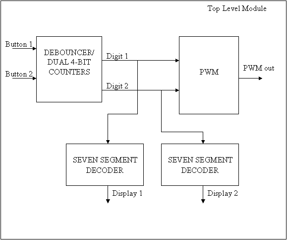
The fourth wrapper module structurally instantiates the three modules described above and connects them together to function as a debounced pulse width modulator with display. Its inputs are the two raw input button signals and a clock signal. Its outputs are the pulse width modulated signal and two seven segment display outputs corresponding to the two 4-bit counters in the debouncer module.
The diagram below shows how the modules are connected together.

Note for interest: This circuit will operate as a DC voltage generator if an RC filter is connected to the PWM output -- when the PWM output is 0, the filter output will be 0V; when the output is a 50% duty cycle, the filter output will be 2.5V; when the output is always high, the filter output will be 5V. And 256 levels can be achieved.
Submit a brief design/testing description, code, and simulation results
for each of the component modules as well as for the module that implements
the entire circuit.
More Bonus (5%):
Change the second module in the bonus section to reduce ripple in the voltage generator. Do this by scrambling the PWM output, but still ensuring that for an input value of x that the output is high x/256 of the time and low (256-x)/256 of the time. (Hint: reverse the bits of the PWM counter).